Scanning Electron Microscope (Sem) / Ultra-High-Resolution Schottky Scanning Electron ... - The scanning electron microscope (sem) is used for observation of specimen surfaces.
Scanning Electron Microscope (Sem) / Ultra-High-Resolution Schottky Scanning Electron ... - The scanning electron microscope (sem) is used for observation of specimen surfaces.. A scanning electron microscope (sem) is a type of microscope which uses a focused beam of electrons to scan a surface of a sample to create a high resolution image. The electrons in the beam interact with the sample, producing various signals that can be used to obtain information about the surface topography and composition. A scanning electron microscope ? An sem is a large piece of scientific equipment that forms detailed images called micrographs, more specifically scanning electron micrographs, of surfaces of extremely small objects called specimens by passing. The sem is a microscope that makes use of electrons as a substitute of sunshine to type an image.
The information below is provided only as a general overview of scanning electron microscopes and the imaging and analysis they can provide. When the specimen is irradiated with a fine electron beam (called an electron probe), secondary electrons are emitted from the specimen surface. With a scanning electron microscope (sem) it is possible to investigate the nano world. Scanning electron microscopy (sem), also known as sem analysis or sem microscopy, is performed with a scanning electron microscope. The scanning electron microscope (sem) is used for observation of specimen surfaces.
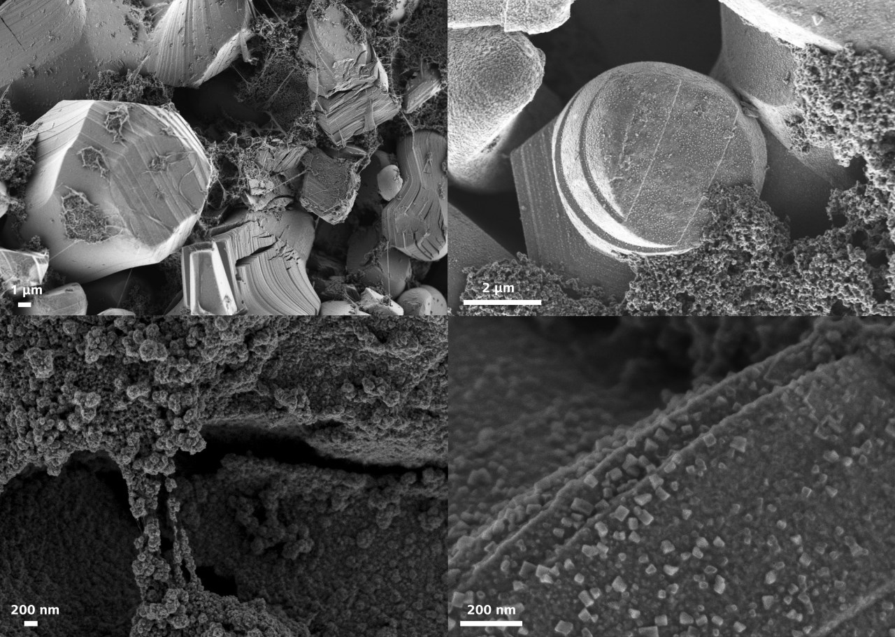
Scanning electron microscopy (SEM) images of (a) PS ... from www.researchgate.net These pollen grains taken on an sem show the characteristic depth of field of sem micrographs. It can be regarded as an effective. Scanning electron microscope flexsem 1000 ii. A electron beam source electronic or magnetic lenses an electron detector and a. A scanning electron microscope (sem) is a type of electron microscope that produces images of a sample by scanning the surface with a focused beam of electrons. A scanning electron microscope (sem), like a transmission electron microscope, consists of an electron optical column, a vacuum system, electronics, and software. The scanning electron microscope (sem) is a type of electron microscope that creates various images by focusing a high energy beam of electrons onto the surface of a sample and detecting signals from the interaction of the incident electrons with the sample's surface. Products / scanning electron microscopes (sem).
A scanning electron microscope (sem) scans a focused electron beam over a surface to create an image.
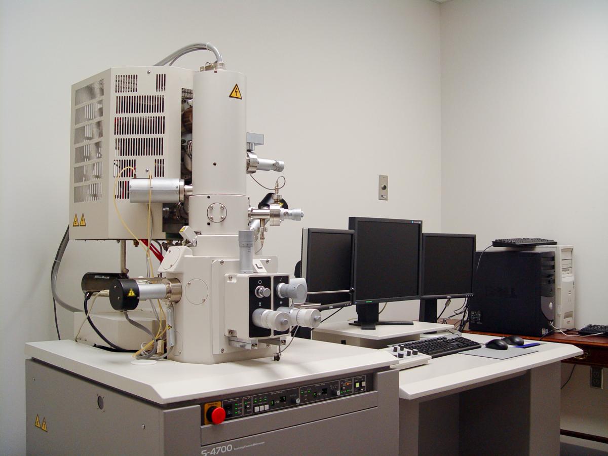
The electrons in the beam interact with the sample, producing various signals that can be used to obtain information about the surface topography and composition. The elements present in the specimens and the elemental composition can be determined. The column is considerably shorter because the only lenses needed are those above the specimen used to focus the electrons. Scanning electron microscope, type of electron microscope, designed for directly studying the surfaces of solid objects, that utilizes a beam of focused electrons of relatively low energy as an electron probe that is scanned in a regular manner over the specimen. The sem is a microscope that makes use of electrons as a substitute of sunshine to type an image. Jump to backscattered electron imaging section. Jeol has played a leading role in the development and evolution of scanning electron microscopes since the early 1960s. Seeing that their development within the early 1950's, scanning electron microscopes have developed new areas of gain knowledge of within the. Products / scanning electron microscopes (sem). Optical microscope, the petrographic microscope and automated optical microscope 1. Advanced electron optical and detection features include immersion mode, beam deceleration mode, and a variety of secondary and backscatter electron detectors (listed below) for. Vacuums are needed to prevent electrical discharge in it is common for the modern sem to be equipped with variable condenser and objective lens apertures. It can be regarded as an effective.
Scanning electron microscopy (sem), which is also recognized as sem analysis or sem. Scanning electron microscope flexsem 1000 ii. Vacuums are needed to prevent electrical discharge in it is common for the modern sem to be equipped with variable condenser and objective lens apertures. Scanning electron microscopy (sem), also known as sem analysis or sem microscopy, is performed with a scanning electron microscope. Products / scanning electron microscopes (sem).
Scanning Electron Microscopy of Lithium-ion Battery ... from blogs.zeiss.com Seeing that their development within the early 1950's, scanning electron microscopes have developed new areas of gain knowledge of within the. Scanning electron microscopy (sem), which is also recognized as sem analysis or sem. Jeol has played a leading role in the development and evolution of scanning electron microscopes since the early 1960s. These pollen grains taken on an sem show the characteristic depth of field of sem micrographs. The information below is provided only as a general overview of scanning electron microscopes and the imaging and analysis they can provide. • the electrons interact with the atoms that make up the sample producing signals that contain information about the. A scanning electron microscope (sem) is a type of electron microscope that produces images of a sample by scanning the surface with a focused beam of electrons. An sem is a large piece of scientific equipment that forms detailed images called micrographs, more specifically scanning electron micrographs, of surfaces of extremely small objects called specimens by passing.
The development of electron microscopes was due to the inefficiency of the wavelength of the light.
A scanning electron microscope (sem), like a transmission electron microscope, consists of an electron optical column, a vacuum system, electronics, and software. Scanning electron microscopes (sems) have become powerful and versatile tools for material characterization, especially in recent years, as the size of materials used in various applications continues to shrink. These pollen grains taken on an sem show the characteristic depth of field of sem micrographs. The scanning electron microscope (sem) is a type of electron microscope that creates various images by focusing a high energy beam of electrons onto the surface of a sample and detecting signals from the interaction of the incident electrons with the sample's surface. A scanning electron microscope (sem) scans a focused electron beam over a surface to create an image. Jeol has played a leading role in the development and evolution of scanning electron microscopes since the early 1960s. It can be regarded as an effective. An sem is a large piece of scientific equipment that forms detailed images called micrographs, more specifically scanning electron micrographs, of surfaces of extremely small objects called specimens by passing. A scanning electron microscope (sem) is a type of electron microscope that produces images of a sample by scanning the surface with a focused beam of electrons. Technique, has been used worldwide in many disciplines. Sem stands for scanning electron microscope. The scanning electron microscope (sem) is used for observation of specimen surfaces. Optical microscope, the petrographic microscope and automated optical microscope 1.
Scanning electron microscopes (sem) scan a sample with a focused electron beam and get images with information about the samples' topography and composition. Primary electrons come from the electron gun situated at the top of the microscope. When combined with scanning probe microscopy (spm), the electron microscope can be used to further control manipulation of nanostructures or select an area. A electron beam source electronic or magnetic lenses an electron detector and a. These pollen grains taken on an sem show the characteristic depth of field of sem micrographs.
Field-Emission Scanning Electron Microscope | Nebraska ... from biotech.unl.edu A electron beam source electronic or magnetic lenses an electron detector and a. It can be regarded as an effective. A scanning electron microscope ? Describe a scanning electron microscope (sem): Sem produces images that can show information on a material's surface composition and topography. Primary electrons come from the electron gun situated at the top of the microscope. The development of electron microscopes was due to the inefficiency of the wavelength of the light. The column is considerably shorter because the only lenses needed are those above the specimen used to focus the electrons.
Sem produces images that can show information on a material's surface composition and topography.
The scanning electron microscope (sem) is a type of electron microscope that creates various images by focusing a high energy beam of electrons onto the surface of a sample and detecting signals from the interaction of the incident electrons with the sample's surface. The elements present in the specimens and the elemental composition can be determined. Scanning electron microscopes (sems) have become powerful and versatile tools for material characterization, especially in recent years, as the size of materials used in various applications continues to shrink. A scanning electron microscope ? With a scanning electron microscope (sem) it is possible to investigate the nano world. A electron beam source electronic or magnetic lenses an electron detector and a. The development of electron microscopes was due to the inefficiency of the wavelength of the light. Jeol has played a leading role in the development and evolution of scanning electron microscopes since the early 1960s. Sem stands for scanning electron microscope. Vacuums are needed to prevent electrical discharge in it is common for the modern sem to be equipped with variable condenser and objective lens apertures. Sem produces images that can show information on a material's surface composition and topography. When combined with scanning probe microscopy (spm), the electron microscope can be used to further control manipulation of nanostructures or select an area. When the specimen is irradiated with a fine electron beam (called an electron probe), secondary electrons are emitted from the specimen surface.
You have just read the article entitled Scanning Electron Microscope (Sem) / Ultra-High-Resolution Schottky Scanning Electron ... - The scanning electron microscope (sem) is used for observation of specimen surfaces.. You can also bookmark this page with the URL : https://murtsii.blogspot.com/2021/05/scanning-electron-microscope-sem-ultra.html
Share Awesome
Belum ada Komentar untuk "Scanning Electron Microscope (Sem) / Ultra-High-Resolution Schottky Scanning Electron ... - The scanning electron microscope (sem) is used for observation of specimen surfaces."
Belum ada Komentar untuk "Scanning Electron Microscope (Sem) / Ultra-High-Resolution Schottky Scanning Electron ... - The scanning electron microscope (sem) is used for observation of specimen surfaces."
Posting Komentar